2022-04-14
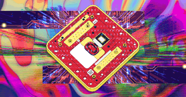
PAM-XIAMEN (Xiamen Powerway Advanced Material Co., Limited) founded in 1990 is a first-class compound semiconductor material enterprise, integrating semiconductor crystal growth, process development and epitaxy, specializing in the research and production of compound semiconductor wafers, such as silicon carbide (SiC) wafer, gallium nitride (GaN) and III-V wafer.
Therein, GaN and SiC belong to the third generation of wide-bandgap semiconductor materials, and the industry chain of both is similar. With the emerging of 5G and electric vehicle market, SiC / GaN have accelerated the research, development and application of related products. PAM-XIAMEN can produce substrates and epitaxial wafers of SiC and GaN.
“The production capability of SiC substrate so far is in 2~6 inch, including N type and semi-insulating type. Also, we grow SiC thin film on SiC substrate for making power devices in electric vehicle (EV). The application of SiC devices in EV is mainly in power control units, inverters, DC-DC converters, on-board chargers, etc. Although the application of silicon carbide in EVs has just started and is still under development, at least one piece of silicon carbide is consumed for every electric vehicle produced, so the development prospect of SiC wafer is broad.” said Victor Chan, general manager of PAM-XIAMEN.
Victor said, “In addition, we grow GaN on SiC substrate, it combines the the excellent thermal conductivity of SiC with the high power density and low loss capability of GaN, ideal for manufacturing radio frequency (RF) and light emitting diode (LED) devices. GaN can be epitaxially on silicon and sapphire in addition to silicon carbide. The GaN on silicon and GaN on sapphire wafers are produced for the fabrication of light emitting diode (LED), RF and power devices. Serving as a semiconductor material solution supplier, our service ability and expertise have been favored by customers.”
Although has numerous customers, PAM-XIAMEN currently intends to ramp up production and enlarge its service capabilities in III-V group substrates and epitaxial wafers, offering high quality solutions, especially in indium antimonide (InSb), gallium antimonide (GaSb), indium phosphide (InP) and gallium arsenide (GaAs) compound wafers.
“The GaAs substrate we grown is by VGF, and it is mainly for epitaxial growth of aluminum gallium arsenide (AlGaAs) and indium gallium arsenide (InGaAs) and etc. And GaAs epi wafers are mainly used for the fabrication of LED, laser diode (LD) and microelectronics. InP is also an important product series and has higher breakdown electric field and thermal conductivity than GaAs, and for InP substrate and epitaxy wafer, LD is the main application,” Victor said, “Furthermore, InSb and GaSb substrate surface quality and flatness from us have approached the level of GaAs and InP substrate, meeting the requirements for the growth of epitaxial materials. Starting this year, we have expanded our ability in grinding, polishing, inspection and cleaning of InSb and GaSb materials. The equipment in our fab is being debugged and running and expected to be put into trial production by the end of the year.”
Company:Xiamen Powerway Advanced Material Co., Limited
Contact Person: Victor
Email: victorchan@powerwaywafer.com
Website: https://www.powerwaywafer.com/
Telephone: +86-592-5601 404
Location:No.77, Lingxia Nan Road, High Technology Zone, Huli, Xiamen